m2c microscopy measurement & calibration m2c microscopy measurement and calibration

Contact Deutsch

News

FIB roughness structure with size of 290 µm x 290 µm on flat Si-substrate (left), on cylindrical NiP surface with radius of about 400 µm (center) and NiP sphere with about 600 µm radius (right)
December 2, 2016

New roughness standards for high resolution measurement techniques

In cooperation with PTB (Physikalisch-Technische Bundesanstalt), m2c developed new roughness standards for high resolution surface measurement techniques. The desired roughness can be selected in an easy way and is used for the production with Focussed Ion Beam (FIB). Repeated profiles, well-known in 2D roughness measurement techniques, are also suitable for this processing technology. For more information, see: PTB Forschungsnachrichten

FIB roughness structure with size of 290 µm x 290 µm on flat Si-substrate (left), on cylindrical NiP surface with radius of about 400 µm (center) and NiP sphere with about 600 µm radius (right)
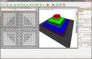
DISS SEM control with Live 3D topography
January 1, 2016

Live 3D Topography

m2c 3D Topography (microShape) is now integrated in the DISS products of point electronic GmbH. This allows the upgrade of your SEM to a complete 3D topographic measurement system.

DISS SEM control with Live 3D topography
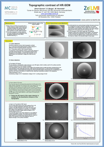
Poster "Topographic contrast of HR-SEM"
October 1, 2015

Best poster award

Ulrich Gernert's (TU Berlin) poster "Topographic contrast of HR-SEM" was awarded with the best poster price (Advances in Instrumentation, Detectors, FIB and Preparation) at the MC 2015 in Göttingen. For the presented evaluation of SEM image data, m2c software was enhanced with special radial histogram analysis.

Poster "Topographic contrast of HR-SEM"